7 Reasons Your Product Failed FCC Part 15 Testing (and How to Fix It)
Failing FCC Part 15 or other radiated emissions standards is more common than most teams expect, especially on first-time designs or complex mixed-signal systems. In almost every case, the root cause is a combination of layout decisions, lack of filtering, grounding problems, and unintended radiation paths that compound each other.
We compiled this list of seven of the most common failure-causing mechanisms that we see, along with practical fixes to consider before you begin your design or PCB layout. Some of these ideas are tried and true, but in other cases, we have found that some long-prescribed practices are no longer recommended.
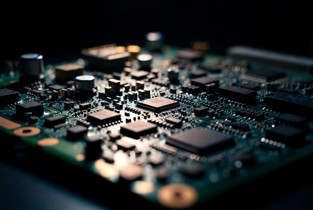
1. Poor PCB Layout and Grounding
Inadequate grounding and poor return path control are among the most frequent causes of radiated emissions failures. PCB grounding is the most fundamental aspect of good RFI/EMI design.
Common issues:
- Broken or discontinuous ground planes
- Long return paths
- High-speed signals crossing plane splits
- Missing bypass caps at each noise source
- No series resistors or ferrites
- No ground floods
Fix:
- Maintain solid, continuous ground planes, as much as possible
- Keep ground return paths directly under signal traces and noise sources
- Avoid routing high-speed signals across gaps or splits in the ground plane
- Avoid using power planes unless absolutely required. This is a holdover from the old days when bypass caps were leaded and multilayer PCBs were insanely expensive. In practice, it causes more problems than it solves.
- Add a bypass cap at each IC and power pin. Caps are so cheap there’s no reason to skimp.
- Add a series resistor or ferrite bead to each noise source to isolate the noise to that component. 10 ohms usually works and is almost free.
- Flood all layers and tie to chassis. There’s no excuse for a PCB with blank areas of substrate and no copper.
2. Cables Acting as Antennas
External cables for power, I/O, and sensor lines often become the dominant radiators during testing. The board may be fine; the cables are doing the broadcasting.
Common issues:
- Long, unfiltered cables
- Poor connector grounding
- No common-mode suppression
Fix:
- Add common-mode chokes where appropriate. Install ferrite on both ground and signal lines to act as a CM choke where possible.
- Improve connector shielding and grounding, design in provisions for a shielded version even if you don’t use it initially.
- Control cable routing and length during testing.
3. Switching Power Supply Noise
Switching regulators are a major source of broadband emissions. If the layout isn’t tight, that noise goes everywhere.
Common issues:
- Poor layout of switching loops
- High di/dt current paths
- Inadequate input/output filtering
Fix:
- Minimize loop area in switching paths as a layout priority, not an afterthought
- Use proper decoupling and bulk capacitance
- Add LC filtering where needed, usually ferrite beads and caps on both input and output
4. Inadequate Shielding
Shielding is often either missing or implemented incorrectly. It costs nothing to add an exposed ground trace around the entire PCB or around noisy circuits now, and you can add a custom shield can later if needed.
Common issues:
- Shields not properly grounded
- Gaps or openings in shielding, especially loose lids and long unsoldered fences
- Floating metal enclosures
Fix:
- Ensure low-impedance connections to ground on all shield elements
- Minimize openings and seams
- Use conductive gaskets where necessary
5. Clock Harmonics and Digital Noise
High-frequency clocks and digital edges generate harmonics that extend well into regulated bands. Edge rate is one of the most underestimated contributors to emissions.
Common issues:
- Excessively fast edge rates
- Poor trace routing
- No filtering or damping on clock lines
Fix:
- Add series resistors for edge-rate control, or switch to a slower device
- Optimize routing of clock lines, bury them on inner layers
- Isolate noisy digital sections from sensitive analog and RF areas
6. Insufficient Filtering
Filters are often missing, incorrectly placed, or improperly designed. And yes – a 100µF electrolytic won’t help at RF. Component selection matters as much as placement.
Common issues:
- Filters placed too far from the noise source
- Incorrect component values
- Ignoring common-mode vs. differential-mode noise
- Wrong type of ferrite or choke for the noise frequencies
- Capacitor too large for the frequency – a 100µF electrolytic won’t help at RF
Fix:
- Place filters close to the source or connector
- Verify filter design for the actual noise type (Common-mode vs. Differential-mode)
- Use proper grounding for all filter components
7. Differences Between Lab Setup and Real Operation
Products often behave very differently in a test lab than in their actual operating environment. If your pre-compliance setup doesn’t match your real-world configuration, you wont get useful data.
Common issues:
- Different cable configurations between pre-compliance and final test
- Test modes not representative of real use
- Unexpected coupling paths in the lab setup
Fix:
- Replicate test lab and real-world conditions during pre-compliance testing
- Test worst-case operating modes, not the most convenient ones
- Evaluate emissions with realistic cable configurations
FCC failures are rarely caused by a single issue. Most problems come from a combination of layout, grounding, and system-level interactions that compound each other. The key to avoiding multiple redesign cycles is identifying the dominant emission source quickly, before you’re at the test lab, ideally during the circuit design and PCB layout phase of the project.
Pre-compliance scanning and targeted design reviews early in the process can significantly reduce time and cost to bring a product to market.
Preparing for compliance testing or working through a failure?
Sanders RF Consulting can help you debug emissions issues, prepare for testing, and get your product across the finish line.